A NAND gate whose inputs come from NAND gates computes an OR of AND terms. Any logic function can be built this way from NAND gates and inverters.
Hint
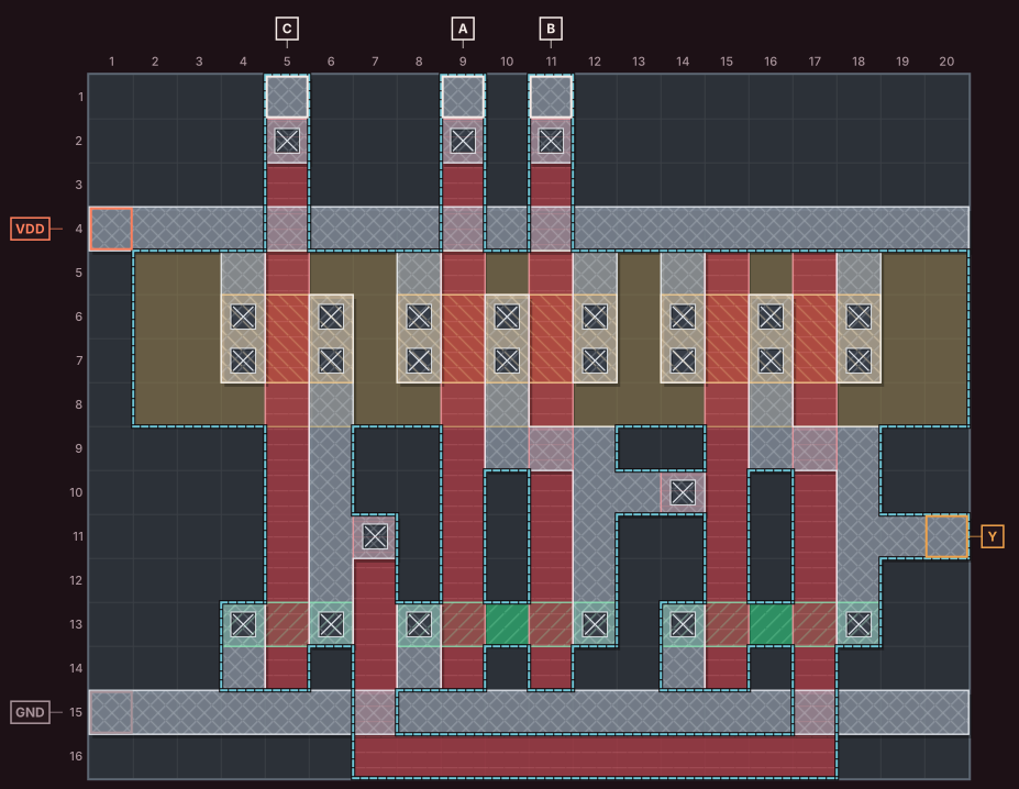
A NAND of two NAND outputs is an OR of two AND terms. Feed one NAND gate with A and B, invert C, and feed both results to a second NAND gate. A line can pass under the GND rail to get around the other gates.
Solution
This is the game's reference drawing for the puzzle. It meets the goal and passes the design rules. Other drawings can pass as well.
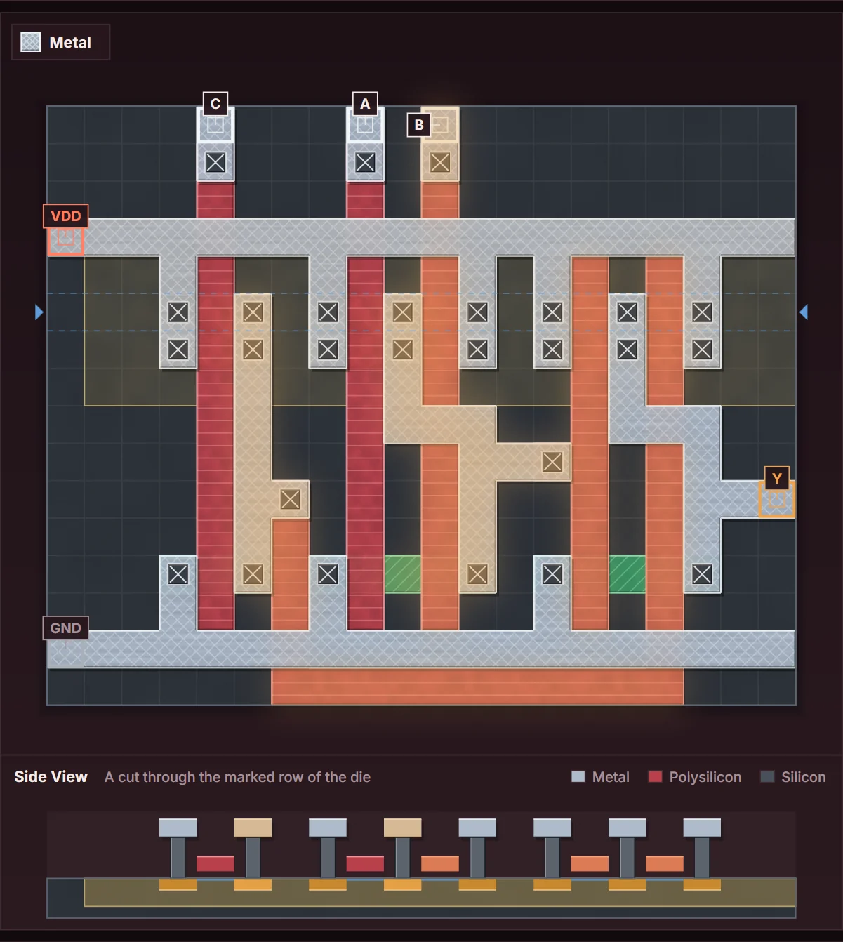
Top View of the solved die, captured from the game. Paths that carry a high level at the moment shown are lit. The Side View below cuts through the row between the dashed lines.The whole game window in Isometric View. The scope on the right compares each output with its target band, and the message above it confirms that the drawing passes.The solution on the grid. Squares are numbered from the top left corner, so you can count them. The dashed outline marks the squares you draw, change, or erase; the rest is drawn when the puzzle opens.
Legend
Metal100 squares
Polysilicon77 squares
Contact27 squares
N active13 squares
P active26 squares
N well76 squares
Input padA, B, C
Output padY
Supply padVDD
Ground padGND
Squares you draw, change, or erase164 squares
About the drawing
The drawing uses 199 of the die's 320 squares.
Part of the drawing is in place when the puzzle opens. To finish it, paint 159 empty squares and change 5 drawn squares.
It forms 10 transistors: 5 N transistors and 5 P transistors. Each one is a place where polysilicon crosses active silicon.
27 contacts join metal to the polysilicon or active silicon under it.
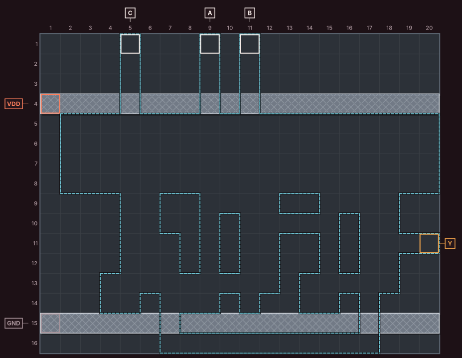
The drawing when the puzzle opens. The dashed outline marks the squares the solution changes.