
Puzzle 14 of 100
CMOS inverter
Goal
Make Y the inverse of A: high while A is low, and low while A is high.
- Die
- 12 by 12 squares
- Layers
- Metal, Polysilicon, Contact, N active, P active, N well
- Input
- A
- Output
- Y
- Supply
- VDD
- Ground
- GND
Guide
- Draw a P transistor near VDD: P active silicon inside an N well, crossed by polysilicon.
- Draw an N transistor near GND, crossed by the same polysilicon line.
- Join one side of each transistor to its rail, and join the other two sides to each other and to Y.
Hint
Hint 1 of 3
Put a P transistor between VDD and Y, and an N transistor between Y and GND. One polysilicon line from A forms both gates.
Hint 2 of 3
Look at the lower transistor, where the input polysilicon crosses active silicon. The marked square is a possible gate location.
Hint 3 of 3
Connect the lower transistor between Y and ground, and the upper transistor between Y and the supply. Connect A to both gates, with contacts away from the crossings.
These hints describe one valid approach. Other drawings can pass.
Solution
This is the game's reference drawing for the puzzle. It meets the goal and passes the design rules. Other drawings can pass as well.
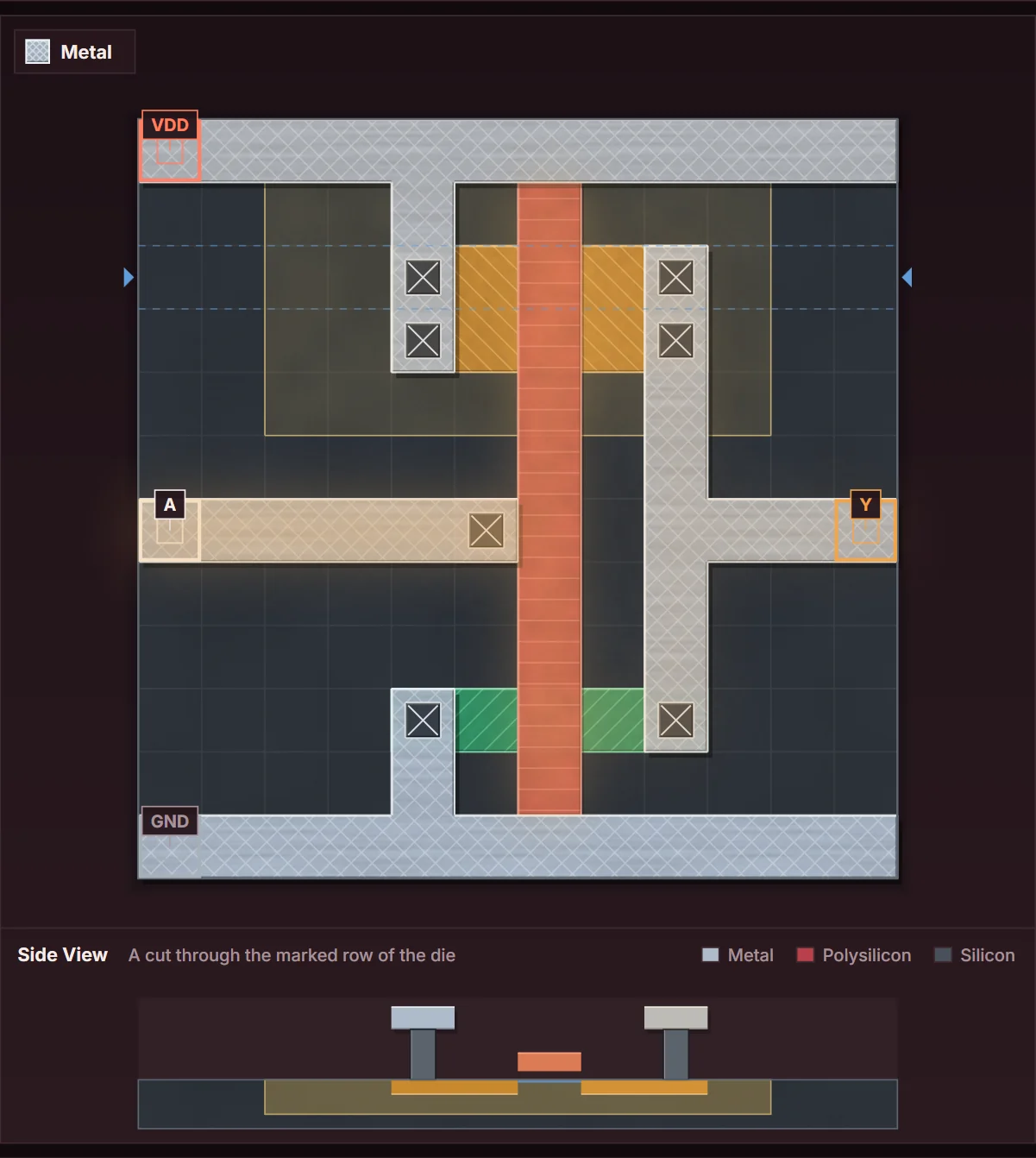
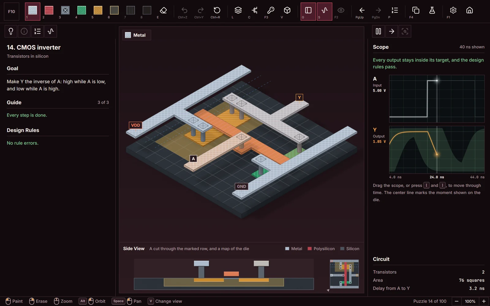
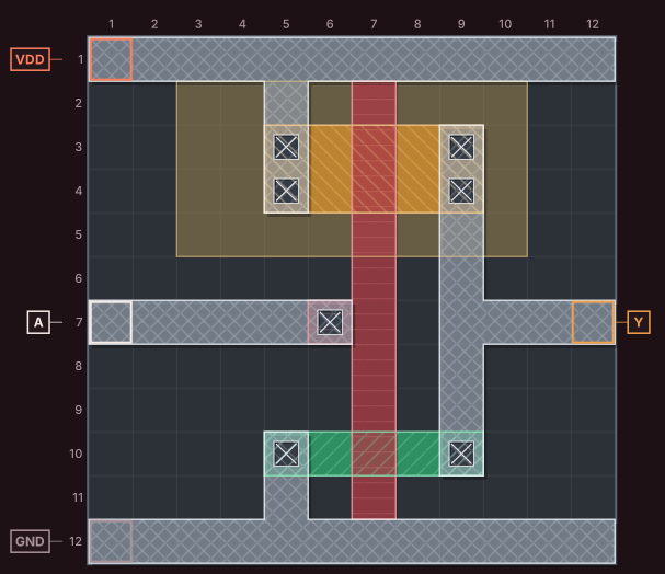
Legend
- Metal46 squares
- Polysilicon11 squares
- Contact7 squares
- N active5 squares
- P active10 squares
- N well32 squares
- Input padA
- Output padY
- Supply padVDD
- Ground padGND
About the drawing
- The drawing uses 80 of the die's 144 squares.
- The die starts empty, so you draw every square.
- It forms 2 transistors: 1 N transistor and 1 P transistor. Each one is a place where polysilicon crosses active silicon.
- 7 contacts join metal to the polysilicon or active silicon under it.
After the puzzle
The output matches an inverter: it goes low when the input is high and high when the input is low, within the allowed transition intervals.
Experiment: Gate width
Before records your passing drawing. Widen one transistor across its gate by extending active silicon beside the existing channel. Extend its source and drain connections if needed, and keep the gate length unchanged. Compare the output delay and edges. Restore Before to undo the experiment, or keep drawing to try another width.
The experiment is optional. It does not change the puzzle target.